PTFA041501GL V1 R250 数据手册
PTFA041501GL
PTFA041501HL
Confidential, Limited Internal Distribution
Thermally-Enhanced High Power RF LDMOS FETs
150 W, 420 – 500 MHz
Description
The PTFA041501GL and PTFA041501HL are 150-watt LDMOS FETs
designed for ultra-linear CDMA power amplifier applications. They
are available in thermally-enhanced plastic open-cavity packages
with copper flanges. Manufactured with Infineon's advanced LDMOS
process, these devices provide excellent thermal performance and
superior reliability.
•
Thermally-enhanced plastic open-cavity (EPOC™)
packages with copper flanges, Pb-free and RoHS
compliant
45
•
Broadband internal matching
40
•
Typical CDMA performance at 470 MHz, 28 V
- Average output power = 60 W
- Linear Gain = 21 dB
- Efficiency = 41%
•
Typical CW performance, 470 MHz, 28 V
- Output power at P–1dB = 175 W
- Efficiency = 62%
•
Integrated ESD protection: Human Body Model,
Class 1 (minimum)
•
Excellent thermal stability
•
Low HCI drift
•
Capable of handling 10:1 VSWR @ 28 V,
150 W (CW) output power
Efficiency
–15°C
25°C
90°C
-35
-40
35
30
-45
25
-50
20
-55
ACPR
15
-60
10
ALT
-65
Drain Efficiency (%)
Adjacent Channel Power Ratio (dB)
VDD = 28 V, IDQ = 900 mA, ƒ = 470 MHz
-30
PTFA041501HL
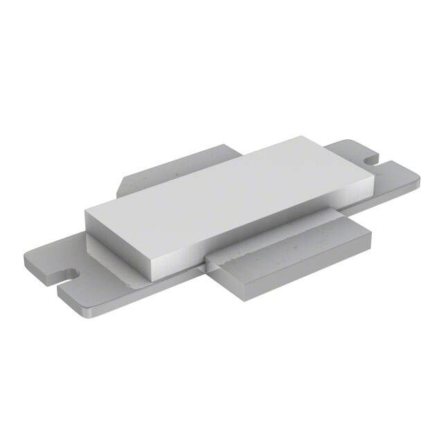
Package PG-64248-2
Features
Single-carrier CDMA IS-95 Performance
-25
PTFA041501GL
Package PG-63248-2
5
-70
-75
0
36
38
40
42
44
46
48
Average Output Power (dBm)
RF Characteristics
Single-carrier CDMA IS-95 Measurements (not subject to production test—verified by design/characterization in
Infineon test fixture)
VDD = 28 V, IDQ = 900 mA, POUT = 60 W average, ƒ = 470 MHz
Characteristic
Symbol
Min
Typ
Max
Unit
Gain
Gps
—
21
—
dB
Drain Efficiency
ηD
—
41
—
%
ACPR
—
–33
—
dB
Adjacent Channel Power Ratio
All published data at TCASE = 25°C unless otherwise indicated
*See Infineon distributor for future availability.
ESD: Electrostatic discharge sensitive device—observe handling precautions!
Data Sheet
1 of 11
Rev. 02, 2008-11-21
�PTFA041501GL
PTFA041501HL
Confidential, Limited Internal Distribution
RF Characteristics (cont.)
Two-tone Measurements (tested in Infineon test fixture)
VDD = 28 V, IDQ = 900 mA, POUT = 150 W PEP, ƒ = 470 MHz, tone spacing = 1 MHz
Characteristic
Symbol
Min
Typ
Max
Unit
Gain
Gps
20.0
21.0
—
dB
Drain Efficiency
ηD
45.0
46.5
—
%
Intermodulation Distortion
IMD
—
–29
–28
dBc
DC Characteristics
Characteristic
Conditions
Symbol
Min
Typ
Max
Unit
Drain-Source Breakdown Voltage
VGS = 0 V, IDS = 10 µA
V(BR)DSS
65
—
—
V
Drain Leakage Current
VDS = 28 V, V GS = 0 V
IDSS
—
—
1.0
µA
On-State Resistance
VGS = 10 V, V DS = 0.1 V
RDS(on)
—
0.07
—
Ω
Operating Gate Voltage
VDS = 28 V, IDQ = 900 mA
VGS
2
2.48
3
V
Gate Leakage Current
VGS = 10 V, V DS = 0 V
IGSS
—
—
1.0
µA
Maximum Ratings
Parameter
Symbol
Value
Unit
Drain-Source Voltage
VDSS
65
V
Gate-Source Voltage
VGS
–0.5 to +12
V
Junction Temperature
TJ
200
°C
Total Device Dissipation
PD
625
W
3.57
W/°C
Above 25°C derate by
Storage Temperature Range
TSTG
–40 to +150
°C
Thermal Resistance (TCASE = 70°C, 150 W CW, soldered)
RθJC
0.28
°C/W
Ordering Information
Type and Version
Package Outline Package Description
Shipping
Marking
PTFA041501GL V1
PG-63248-2
Thermally-enhanced slotted flange,
single-ended
Tray
PTFA041501GL
PTFA041501HL V1
PG-64248-2
Thermally-enhanced slotted flange,
single-ended
Tray
PTFA041501HL
*See Infineon distributor for future availability.
Data Sheet
2 of 11
Rev. 02, 2008-11-21
�PTFA041501GL
PTFA041501HL
Confidential, Limited Internal Distribution
Typical Performance (data taken in a production )
POUT, Gain & Efficiency (at P-1dB) vs. Frequency
Broadband Circuit Performance
VDD = 28 V, IDQ = 900 mA, P–1dB
45
-14
Efficiency
40
-15
35
-16
Return Loss
30
-17
-18
Gain
20
60
55
462
464
466
45
20.5
40
20.4
35
20.3
20.2
30
Gain
20.1
20
15
460
462
Frequency (MHz)
19.9
470
468
Power Sweep, CW Conditions
VDD = 28 V, ƒ = 470 MHz
VDD = 28 V, IDQ = 900 mA, ƒ = 470 MHz
21.0
20.5
19.5
IDQ = 900 mA
19.0
22
80
21
70
20
IDQ = 1125 mA
20.0
Gain (dB)
Gain (dB)
466
Power Sweep at selected IDQ
21.5
60
Gain
19
50
18
40
Efficiency
17
IDQ = 675 mA
18.0
464
Frequency (MHz)
22.0
18.5
20.6
P–1dB
20
-20
470
468
20.7
50
25
-19
15
460
20.8
Efficiency
30
TCASE = 25°C
TCASE = 90°C
16
17.5
17.0
20
15
39
41
43
45
47
49
51
53
55
Data Sheet
10
39
Output Power (dBm)
Drain Efficiency (%)
25
20.9
Gain (dB)
-13
Efficiency (%), P1dB
(dBm)
50
65
Input Return Loss (dB)
Gain (dB), Efficiency (%)
VDD = 28 V, IDQ = 900 mA, P1dB
41
43
45
47
49
51
53
55
Output Power (dBm)
3 of 11
Rev. 02, 2008-11-21
�PTFA041501GL
PTFA041501HL
Confidential, Limited Internal Distribution
Typical Performance (cont.)
Intermodulation Distortion vs. Pout
IM3 vs. Output Power at Selected Biases
VDD = 28 V, IDQ = 900 mA,
VDD = 28 V , ƒ1 = 469 MHz, ƒ 2 = 470 MHz
0
50
-25
-10
45
-27
40
Efficiency
35
-30
IM3
30
-40
25
IM5
-50
20
-60
IM7
-70
36
38
40
42
44
46
48
675 mA
-29
IMD (dBc)
-20
Drain Efficiency (%)
Intermodulation Distortion (dBc)
ƒ 1 = 469 MHz, ƒ 2 = 470 MHz
-31
-33
900 mA
-35
-37
1125 mA
-39
15
-41
10
-43
36
50
38
Output Power (dBm), avg.
42
44
46
48
Bias Voltage vs. Temperature
Voltage normalized to typical gate voltage,
series show current
IDQ = 900 mA, ƒ = 470 MHz
55
0.29 A
Normalized Bias Voltage (V)
1.03
54
53
52
51
26
28
30
32
1.47 A
1.01
2.20 A
1.00
4.41 A
0.99
6.61 A
8.81 A
0.98
11.02 A
0.97
0.96
0
20
40
60
80
100
Case Temperature (°C)
Supply Voltage (V)
Data Sheet
0.88 A
1.02
0.95
-20
50
24
50
Output Power (dBm)
Output Power (at 1 dB Compression)
vs. Supply Voltage
Output Power (dBm)
40
4 of 11
Rev. 02, 2008-11-21
�PTFA041501GL
PTFA041501HL
Confidential, Limited Internal Distribution
RD G
Broadband Circuit Impedance
S T OW
A
Z Source Ω
Frequency
Z Load Ω
MHz
R
jX
R
jX
450
0.88
–3.20
1.33
0.22
455
0.84
–3.20
1.35
0.31
460
0.84
–3.10
1.40
0.38
465
0.84
–3.00
1.41
0.47
470
0.83
–2.90
1.44
0.57
0.2
0.1
0.0
470 MHz
450 MHz
Z Source
470 MHz
450 MHz
0.1